![]()
LED chip principle and basic knowledge

I. Brief History of LED
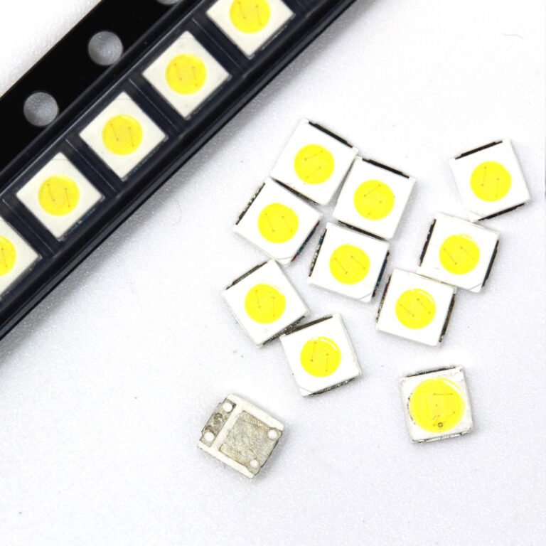
The basic knowledge that semiconductor materials can generate light has been recognized by people as early as 50 years ago. In 1962, Nick Holonyak Jr. of General Electric successfully developed the first visible light emitting diode used in practice. LED is the abbreviation of light emitting diode in English. Its basic structure is a piece of electroluminescent semiconductor material. It is placed in a shelf with leads and then sealed with epoxy resin around it, which is a solid package. Therefore, it can protect the internal core wire and make the LED have good shock resistance.
Initially, LEDs were used as indicator light sources for instruments and meters. Later, various light-colored LEDs were widely used in traffic lights and large-area displays, producing good economic and social benefits. Taking a 12-inch red traffic light as an example, in the United States, long-life, low-efficiency 140-watt incandescent lamps were originally used as light sources, producing 2000 lumens of white light. After passing through a red filter, the light loss is 90%, leaving only 200 lumens of red light. In the newly designed lamp, Lumileds company uses 18 red LED light sources, including circuit losses, which consume a total of 14 watts to produce the same light effect. Car signal lights are also an important area for the application of LED light sources.
II. Principle of LED chip
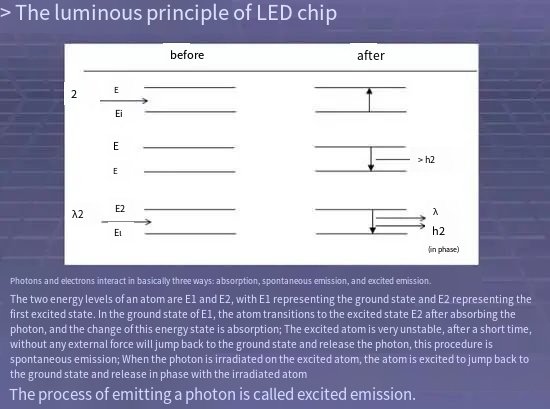
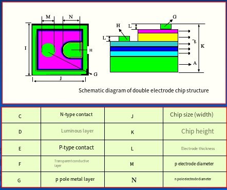
An LED (Light Emitting Diode) is a semiconductor device which converts electrical current directly into light. At the core of an LED is a semiconductor chip connected to either an attachment point or to the positive pole of its power supply, and then sealed in epoxy resin encasing. A semiconductor chip consists of two main parts, with one consisting of a p-type semiconductor where holes predominate and another being an n-type semiconductor where electrons do. When these two semiconductors come into contact, a “P-N junction” occurs and has to be avoided at all costs. Current flowing through a wire and acting on the chip pushes electrons into the P region of an LED chip, where electrons follow holes to recombine and emit photons as energy as photons; this process produces LED light emission; its wavelength or color depends on which materials make up its P-N junction junctions.


Ⅲ. Classification of LED Chips
1. Definition and characteristics of MB chip
Definition: Metal Bonding chip; this chip is a patented product of UEC.
Features: (1) High thermal conductivity material, Si, is used as the substrate, making heat dissipation easy. Thermal Conductivity: GaAs: 46W/m-K; GaP: 77W/m-K; Si: 125-150W/m-K; Cupper: 300-400W/m-k; SiC: 490W/m-K (2) The epitaxial layer and substrate are bonded through a metal layer (wafer bonding), while reflecting photons to avoid absorption by the substrate. (3) The conductive Si substrate replaces the GaAs substrate, with good thermal conductivity (thermal conductivity difference of 3-4 times), making it more suitable for high drive current applications. (4) The bottom metal reflective layer is beneficial for improving luminosity and heat dissipation. (5) The size can be increased for applications in high power fields, eg: 42mil MB.
2. Definition and characteristics of GB chip
Definition: Glue Bonding chip; this chip is a patented product of UEC.
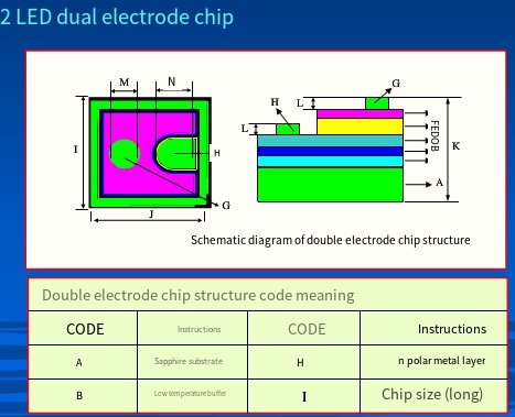
Features: (1) Transparent sapphire substrate replaces the light-absorbing GaAs substrate, with a light output power more than twice that of traditional AS (Absorbable structure) chips, and the sapphire substrate is similar to the GaP substrate of TS chips. (2) The chip emits light from all sides, with excellent patterning. (3) In terms of brightness, its overall brightness has exceeded the level of TS chips (8.6mil). (4) Dual electrode structure, which is slightly inferior to TS single electrode chips in terms of high current resistance.
3. Definition and characteristics of TS chip
Definition: transparent structure chip, which belongs to HP’s patented product.
Features: (1) The chip technology is complex and far superior to AS LED. (2) Excellent reliability. (3) Transparent GaP substrate, no light absorption, high brightness. (4) Wide range of applications.
4.Definition and characteristics of AS chip
Definition: Absorbable structure (absorbing substrate) chip; through nearly four decades of development and efforts, Taiwan’s LED optoelectronic industry is in a mature stage of development, production, and sales of such chips, and the research and development levels of major companies in this area are basically the same, with little difference.
The chip manufacturing industry in mainland China started late, and there is still a certain distance between its brightness and reliability compared to Taiwan’s industry. In this article, AS chips specifically refer to AS chips in UEC, eg: 712SOL-VR, 709SOL-VR, 712SYM-VR, and 709SYM-VR.
Features: (1) Quad chip, prepared using MOVPE technology, with higher brightness than conventional chips. (2) Excellent reliability. (3) Wide range of applications.
IV. the types of LED chip materials
1. LPE: Liquid Phase Epitaxy GaP/GaP
2. VPE: Vapor Phase Epitaxy (VPE) GaAsP/GaAs
3. MOVPE: Metal Organic Vapor Phase Epitaxy (MOVPE) AlGaInP, GaN
4. SH: GaAlAs/GaAs Single Heterostructure
5. DH: GaAlAs/GaAs Double Heterostructure
6.DDH: GaAlAs/GaAlAs Double Heterostructure
V. Composition and Luminescence of LED Chips
1. Composition of LED chip:
It mainly consists of several elements such as arsenic (As), aluminum (Al), gallium (Ga), indium (In), phosphorus (P), nitrogen (N), and strontium (Si).
2. Classification of LED chips:
(1) Classified by luminance:
A. General brightness: R, H, G, Y, E, etc
B. High brightness: VG, VY, SR, etc
C. Ultra-high brightness: UG, UY, UR, UYS, URF, UE, etc
D. Invisible light (infrared): R, SIR, VIR, HIR
E. Infrared receiver tube: PT
F. Photoelectric cell: PD
(2) By component elements:
A. Binary wafer (phosphorus, gallium): H, G, etc
B. Ternary chips (phosphorus, gallium, arsenic): SR, HR, UR, etc
C. Quaternary wafer (phosphorus, aluminum, gallium, indium): SRF, HRF, URF, VY, HY, UY, UYS, UE, HE, UG