![]()
Three Structures of LED Chips
From the perspective of structure, LED chip types are mainly divided into front-side chip, flip chip and vertical chip.
Regular LED chip
Part1
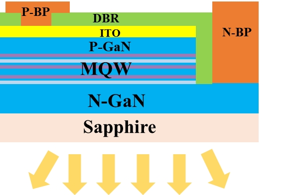
Formal LED chip structure
The LED normal chip structure was one of the first ever developed. From top to bottom: electrode, P-type semiconductor layer, light emitting layer, N-type semiconductor layer and substrate. All heat generated at PN junction must pass through sapphire substrate before reaching heat sink; its poor thermal conductivity resulting in reduced output and reliability of chip.
Part2
Advantages and Disadvantages of Regular LED Chips
Advantages: The structure is simple and the manufacturing process is relatively mature;
Disadvantages:
(1) The p- and n-electrodes of the forward-structured LED are located on the same side of the LED, and the current must flow laterally through the n-GaN layer, resulting in current congestion and localized heat generation, which limits the driving current;
(2) The poor thermal conductivity of sapphire substrates severely hinders heat dissipation.
(3) Temperature and humidity can cause electrode metal migration. As the chip size shrinks, the distance between the positive and negative electrodes decreases, which can lead to short-circuit problems.
Part3
Classification of Formal LED Chip
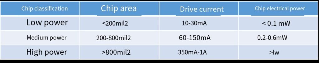
There are many ways to classify the chip, such as light color, chip power, application range, etc. In order to better explain the structure of the chip, this article divides the chip into three categories: low-power chip, medium-power chip, and high-power chip based on the chip power. (At present, the LED industry has not strictly defined the three types of power chips, and the following table is for reference only.)
Part4
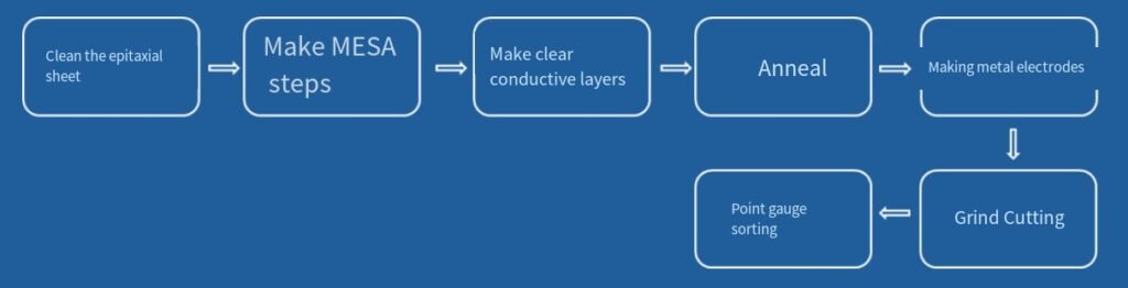
Preparation process of positive LED chip
(1) Small power chip:
The structure of low-power chips is relatively simple, and the manufacturing process is also relatively simple. Typically, three photolithographic processes are used, namely MESA lithography, ITO lithography, and PAD lithography. The detailed process is as follows:
(2) Medium-power chip:
The medium-power chip usually adopts 5 times of lithography process, which adds current blocking layer (CBL) lithography and passivation (PV) lithography on the basis of the 3 times of lithography process for low-power. The specific process flow is as follows:

The process flow of ITO followed by MESA can also be adopted, which is beneficial to the improvement of chip yield. The detailed process flow is as follows:

After grinding, medium-power chips are usually back-plated with a high-emissivity DBR. The DBR can significantly improve the brightness of the chip’s point measurement, and also has a certain improvement on the brightness of the packaged chip.
(3) High-power chip
High-power chips usually also use medium-power 5-step lithography processes, but the back plating layer will be changed from the original DBR to an ODR (omnidirectional reflective layer).
Part5
Application Status of Formal LED Chip
The sapphire-substrate structure has been the mainstream structure for GaN-based LEDs due to its simple process and relatively low cost. Currently, most companies still use this structure to save production and research and development costs.
Flip-chip LED chip
Part1
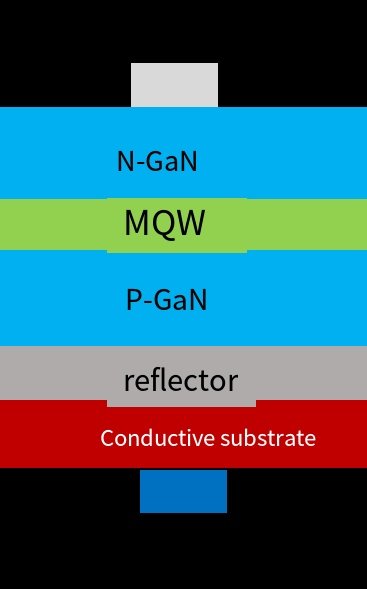
Flip-chip LED chip structure
The flip chip structure consists of a sapphire substrate, an N-type semiconductor light-emitting layer, a P-type semiconductor layer, and an electrode, from top to bottom. Compared to the flip chip structure, the heat generated at the PN junction in this structure can be directly conducted to the heat sink without passing through the substrate. In the flip structure, both the p-electrode and n-electrode are on the bottom surface, avoiding the obstruction of emitted light and improving light emission efficiency.
Part2
Advantages and disadvantages of flip-chip LED chips:
Advantages:
(1) Without using sapphire for heat dissipation, heat from the PN junction of the chip is transferred to the Si heat sink through gold wire bumps. Si is a good conductor for heat dissipation, and its cooling effect is far better than that of sapphire, allowing for high-current use;
(2) The size can be made smaller, the density can be higher, and the optical matching is easier;
(3) The heat dissipation function is improved, which extends the life of the chip; (4) The anti-static ability will also be improved;
(5) Lay a foundation for the subsequent packaging process;
The distance between the electrodes is relatively large, which can reduce the risk of short circuit caused by electrode metal migration.
Disadvantages:
(1) At present, flip-chip LED technology has greater advantages in high-power products and integrated packaging, but its cost competitiveness is not very strong in small and medium-power applications.
(2) Inverted LEDs subvert traditional LED processes, from chips to packaging, which requires higher equipment requirements.
Part3
Preparation process of flip-chip LED chip

The preparation process flow of flip-chip LED chips is shown in the figure below:
Part4
Application Status of Flip-chip LED
At present, due to the high requirements for manufacturing equipment and costs, there are relatively few manufacturers of such chips. Therefore, although the market application is not very extensive, it has a very broad prospect.
Vertical LED chip
Part1
Vertical LED chip structure
Using high thermal conductivity substrates (Si, Ge, Cu, etc.) instead of sapphire substrates greatly improves the heat dissipation of the chip.
Part2
Advantages and disadvantages of vertical LED chips:
Advantages:
At present, all existing color vertical structure LEDs: red LEDs, green LEDs, blue LEDs, and ultraviolet LEDs can be made into through-hole vertical structures;
(2) All manufacturing processes are carried out at the wafer level;
(3) Due to the elimination of the need to connect gold wires to external power sources, the packaging thickness of LED chips with through-hole vertical structures has been reduced;
(4) Strong antistatic ability;
(5) Larger diameter through-holes/metal fill plugs and multiple through-holes/metal fill plugs can be used to further improve the heat dissipation efficiency of the substrate.
Disadvantages: complex process and low production pass rate.
Part3
The preparation process of vertical LED chips

The process of preparing GaN-based vertical structure LEDs mainly consists of the following steps: surface treatment, mesa etching, passivation layer deposition, etc. The specific process is as follows:
Part4
Application Status of Vertical LED Chip:
Vertical structure blue chip is produced on the basis of normal assembly. This chip reverses the traditional sapphire substrate chip and bonds it on a silicon substrate or metal substrate with good thermal conductivity, and then laser strips the sapphire substrate. This structure of chip solves the problem of heat dissipation, but due to the complex process and low production yield, it is currently developing at a slow pace.